

Планиране на FPGA.

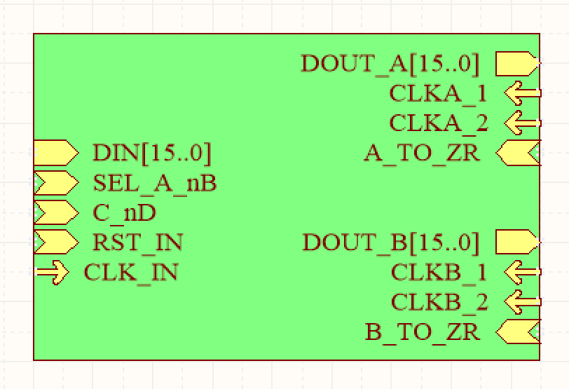
Както споменах, FPGA след като го заредим със съответният двоичен стрийм се превръща в цифрова интегрална схема с желана от нас функционалност. На прикрепената към публикацията снимка са отразени входовете и изходите на “желаната от нас интегрална схема”. От лявата страна са изводите които управляват входа на данните в схемата, а от дясната тези които управляват изхода. Може да забележите, че имаме два изхода ( можем да синтезираме едновременно два изходни сигнала - A и B). Това е с оглед на максималното използване на ресурсите на чипа. Ако го конфигурираме като 16 битова памет от наличните ресурси можем да извлечем 4096 клетки. Ако обаче това го разделим на две пространства ще имаме по 2048 клетки. Приемаме, че синтезираме най-често използваната функция - синус, тогава 360/2048 = 0,17578125 - части от градуса. Ех, ако бях някой педант сега трябваше да проверя при около 90°, колко е нарастването с така получената от нас стойност - защото това ще е максималната грешка от дискретизация, но оставям това на вас. Следва описание на входовете и изходите по функционалност:
Изходна страна A:
DOUT_A[15..0] - изходи на които се извежда 16 битовата информация записана в блок A на двупортовата памет. Свързват се към съответната R-2R матрица и така формираме аналоговият сигнал. Стойността записана в клетката избрана от адресният брояч се извежда по ПРЕДЕН фронт на вътрешният тактов сигнал
CLKA_1 и CLKA_2 - входове, правят вътрешен XOR, идеята е при подаване на два, дефазирани на 90 градуса тактови импулса да получим удвоена тактова честота. Ако подаваме само един импулс, независимо от логическото ниво на другият - тактовата честота остава като тази на импулса. С тази тактова честота се инкрементира 11 битов кръгов брояч който се свързва към адресните входове на паметта. Броячът увеличава стойността си по ЗАДЕН фронт на тактовият сигнал
A_TO_ZR - вход, при високо входно ниво извежда логическа 0 на изходите DOUT , преминаването от високо към ниско ниво (заден фронт) нулира адресният брояч, задържането на сигнала в ниско ниво разрешава извеждането на съдържанието на паметта според съответният адрес.
Изходна страна B: Същите като на страна A.
Входна страна:
DIN[15..0] - входове за данни, според сигнала SEL_A_nB данните се записват съответно в страна A или B, при ПРЕДЕН фронт на тактовият сигнал CLK_IN.
SEL_A_nB – при високо ниво входовете се отнасят за страна A, при ниско за страна B
C_nD - с този сигнал избираме режим конфигурация или режим запис на данни. При високо ниво е избран режим конфигурация, данните се записват във вътрешен регистър съответно за страна A или B и числото записано в този регистър служи за делител на тактовата чистота с която данните се извеждат, целта е да можем да получим ниски честоти на изходният сигнал, а не само високи. При ниско ниво се осъществява запис от входовете DIN[15..0] във съответно избраната част от паметта посредством сигналите SEL_A_nB и CLK_IN
RST_IN – при високо ниво нулира адресният брояч на входа и не позволява увеличаването му, при ниско разрешава работата му.
CLK_IN – входен тактов сигнал, при ниско ниво на RST_IN и заден фронт инкрементира входният адресен брояч и така се формира адреса на клетката в която ще записваме на избраната със сигнал SEL_A_nB страна. При нисък RST_IN и преден фронт записва съответната клетка. За да се изпълнява всичко това е необходимо сигналът C_nD да е с ниско логическо ниво. При високо логическо ниво на C_nD, стойността на адресният брояч не се взема под внимание и при заден фронт на сигнала CLK_IN извършваме запис в избраният с SEL_A_nB КОНФИГУРАЦИОНЕН РЕГИСТЪР.
06-03-2026
FPGA Planning.
 As I mentioned, after loading it with the corresponding binary stream, the FPGA becomes a digital integrated circuit with the functionality we want. The photo attached to the publication shows the inputs and outputs of the “desired integrated circuit”. On the left side are the pins that control the data input into the circuit, and on the right are those that control the output. You may notice that we have two outputs (we can synthesize two output signals simultaneously - A and B). This is in view of the maximum use of the chip's resources. If we configure it as a 16-bit memory, we can extract 4096 cells from the available resources. However, if we divide this into two spaces, we will have 2048 cells each. We assume that we synthesize the most commonly used function - sine, then 360/2048 = 0.17578125 - parts of a degree. Well, if I were a pedant now I would have to check at about 90°, how much is the increase with the value we obtained in this way - because this will be the maximum error from discretization, but I leave that to you. The following is a description of the inputs and outputs by functionality:
Output side A:
DOUT_A[15..0] - outputs that output the 16-bit information recorded in block A of the two-port memory. They are connected to the corresponding R-2R matrix and thus we form the analog signal. The value recorded in the cell selected by the address counter is output on the LEFT edge of the internal clock signal
CLKA_1 and CLKA_2 - inputs, make an internal XOR, the idea is that when two, 90-degree phase-shifted clock pulses are supplied, we get a doubled clock frequency. If we supply only one pulse, regardless of the logic level of the other - the clock frequency remains the same as that of the pulse. With this clock frequency, an 11-bit circular counter is incremented, which is connected to the address inputs of the memory. The counter increases its value on the TRAILING edge of the clock signal
A_TO_ZR - input, at a high input level, it outputs a logical 0 at the DOUT outputs, the transition from high to low level (trailing edge) resets the address counter, keeping the signal at a low level enables the output of the memory contents according to the corresponding address.
Output side B: The same as on side A.
Input side:
DIN[15..0] - data inputs, according to the SEL_A_nB signal, the data is written to side A or B, respectively, at the TRAILING edge of the CLK_IN clock signal.
SEL_A_nB - at a high level, the inputs refer to side A, at a low level to side B
C_nD - with this signal we select configuration mode or data recording mode. At high level, configuration mode is selected, data is written to an internal register for side A or B respectively and the number written in this register serves as a divisor of the clock purity with which the data is output, the goal is to be able to obtain low frequencies of the output signal, not only high ones. At low level, writing is performed from the DIN[15..0] inputs in the respectively selected part of the memory by means of the SEL_A_nB and CLK_IN signals
RST_IN – at high level, the address counter of the input is reset and does not allow its increase, at low level, it enables its operation.
CLK_IN – input clock signal, at low level of RST_IN and a trailing edge, the input address counter is incremented and thus the address of the cell in which we will write on the side selected with the SEL_A_nB signal is formed. At low RST_IN and a leading edge, the corresponding cell is written. In order to perform all this, it is necessary for the C_nD signal to be at a low logic level. At a high logic level of C_nD, the value of the address counter is not taken into account and at the falling edge of the CLK_IN signal we write to the CONFIGURATION REGISTER selected with SEL_A_nB.
06-03-2026
Ядрото на ядрото / The Core of the Core
Вече споменах, че ще гледам да избягвам подробните обяснения, а ще наблегна на конкретни резултати. Може също да съм споменал, че принципно за мене си съм изяснил как структурно ще изглежда генератора, просто не бързам с реализацията, за мен това не е проект който ще ме изхранва и работя по него само когато почувствам вътрешна нужда от това, така удоволствието е най-голямо. Темата на днешната публикация е “Ядрото на ядрото” и ще се опитам да обясня защо. Ядрото на устройството ще бъде FPGA интегрална схема. В нея, чрез съответната конфигурираща програма се създава логическа структура която с помощта на външните резистори ще синтезира необходимият ни сигнал. И така, за да осъществим това ни е необходима така наречената двупортова памет и тя е ядрото на останалата логическа структура която ще създадем и ще бъде ядрото на устройството. С опреснени познания в VHDL програмирането създаваме двупортовата памет и съответно я тестваме със симулатора. Изходният програмен код можете да ИЗТЕГЛИТЕ от тук. На приложената снимка се виждат отделните етапи от теста, при създаването си двупортовата памет съдържа семплите на синусоида, няколко такта след като започваме да извеждаме синусоидата започваме със въвеждането на триъгълника, и после съответно извеждаме и него. И така като възможности имаме 2048, 16 битови семпъла за синтез на желаният от нас сигнал. От втората екранна снимка може да се види интегралната схема на която съм избрал и резултатите от синтеза на програмата.
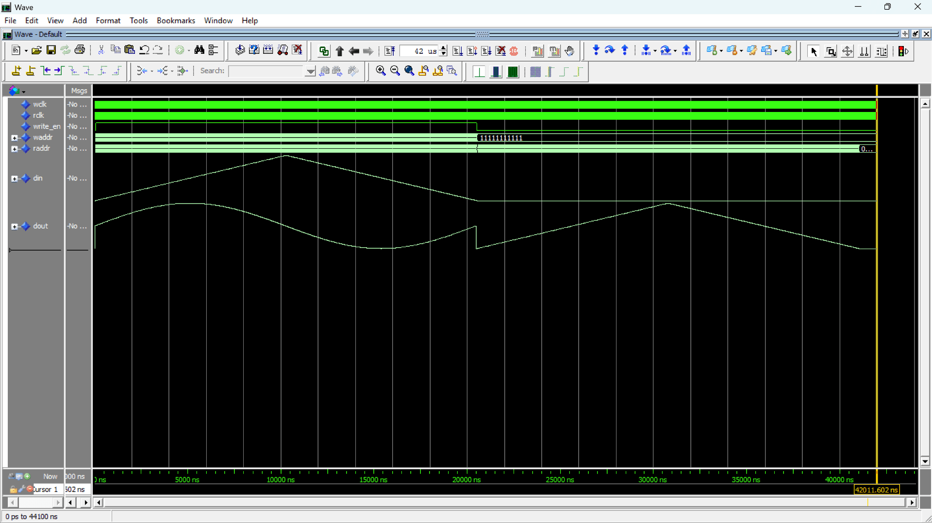
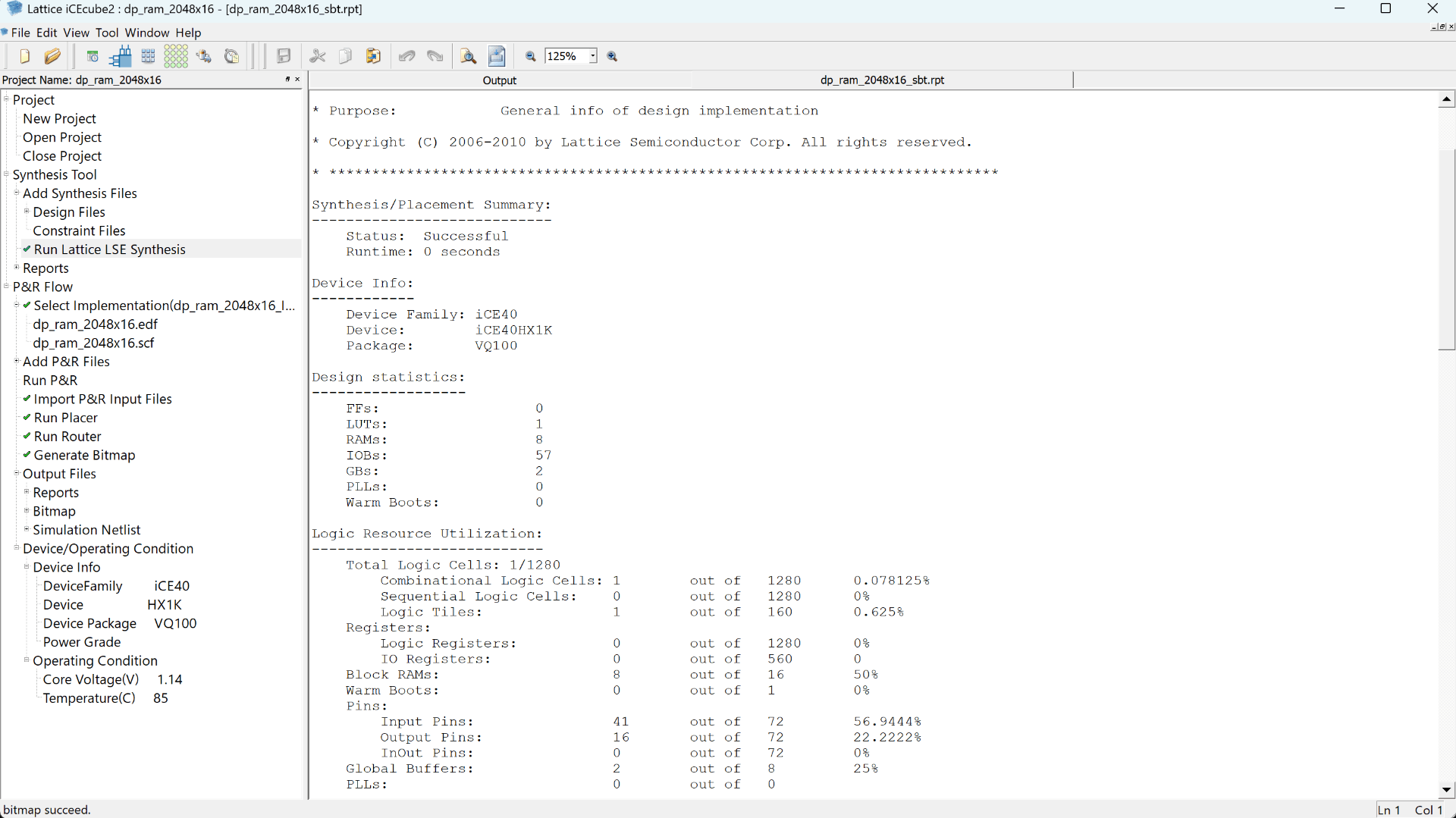
I have already mentioned that I will try to avoid detailed explanations, and will emphasize specific results. I may also have mentioned that in principle I have clarified for myself how the generator will look structurally, I am just not in a hurry with the implementation, for me this is not a project that will feed me and I work on it only when I feel an internal need for it, that is the greatest pleasure. The topic of today's publication is “The Core of the Core” and I will try to explain why. The core of the device will be an FPGA integrated circuit. In it, through the corresponding configuration program, a logical structure is created which, with the help of external resistors, will synthesize the signal we need. So, to achieve this we need the so-called two-port memory and it is the core of the remaining logical structure that we will create and will be the core of the device. With refreshed knowledge in VHDL programming, we create the two-port memory and accordingly test it with the simulator. You can DOWNLOAD the source code from here. The attached picture shows the individual stages of the test, when created the two-port memory contains the samples of a sine wave, a few cycles after we start outputting the sine wave, we start inputting the triangle, and then we output it accordingly. And so as possibilities we have 2048, 16 bit samples for synthesis of the signal we want. From the second screenshot you can see the integrated circuit that I have chosen and the results of the program synthesis.
28-10-2025
VHDL приключения / VHDL adventures
На тази страница, както съм планирал преди години започвам публикуването на това как да си направим генератор на сигнали. За разлика от страницата където се постарах да опиша максимално подробно направата на регулируемото захранване, тук ще гледам да съм по кратък и да публикувам основно резултати. Все пак проекта е предназначен за доста по напреднали в електрониката. Основните умения които ще са ви необходими са запояване на SMD компоненти и запис на фърмуер в микроконтролер STM32. Другата разлика от останалите страници на сайта е, че публикациите по дати ще са наобратно - първо най новите, а на края най старите. Така е организирана CMS системата (добавя новите раздели в публикацията най отгоре) и за мен е по лесно да я ползвам така. Структурно проекта ще е изпълнен на две платки с размери не по големи от 10х10 сантиметра - това са размерите които приемат производителите на печатни платки по преференциални цени. На едната платка ще са енкодерите, микроконтролера, FPGA, няколко операционни усилвателя за буфериране и управление на офсета и управляем генератор на тактова честота за FPGA . На другата платка ще са стабилизаторите на напрежение, изправителите и изходните усилватели на двата канала. Изхождайки от това съм избрал ТАЗИ КУТИЯ (ако линка спре да работи търсите - 0905 Case). Поста нарекох VHDL приключения защото имах доста такива докато получа лиценз за програмата iCEcube2 – обявена като свободна за хобисти. Наложи се доста да им пиша, обяснявам и т.н. В края на краищата имам лиценз за една година и ще гледам в рамките на този период да приключа с нещата по програмирането на FPGA чипа. ПРОГРАМАТА която написах просто прогонва цялата верига от инструменти за това - така знам, че имам всичко работещо. Също така с помощта на изкуственият интелект си направих ФОРМА ЗА ПОДБОР НА РЕЗИСТОРИТЕ които свързани в изходите на FPGA ще формират изходните напрежения (по таблица изчислена и заредена от микроконтролера) на двата канала.
On this page, as I planned years ago, I start publishing how to make a signal generator. Unlike the page where I tried to describe in as much detail as possible the making of the adjustable power supply, here I will try to be brief and mainly publish results. After all, the project is intended for much more advanced electronics users. The main skills you will need are soldering SMD components and writing firmware to an STM32 microcontroller. The other difference from the other pages of the site is that the publications by date will be in reverse - the newest first, and the oldest at the end. This is how the CMS system is organized (it adds new sections to the publication at the top) and it is easier for me to use it that way. Structurally, the project will be implemented on two boards with dimensions no larger than 10x10 centimeters - these are the dimensions that printed circuit board manufacturers accept at preferential prices. On one board will be the encoders, microcontroller, FPGA, several operational amplifiers for buffering and offset control and a controllable clock generator for the FPGA. On the other board will be the voltage stabilizers, rectifiers and output amplifiers of both channels. Based on this, I have chosen THIS BOX (if the link stops working, search for - 0905 Case). I called the post VHDL adventures because I had quite a few of them while I was getting a license for the iCEcube2 program - announced as free for hobbyists. I had to write to them a lot, explain, etc. After all, I have a license for a year and I will try to finish the programming of the FPGA chip within this period. THE PROGRAM I wrote simply drives away the entire chain of tools for this - that's how I know that I have everything working. Also, with the help of artificial intelligence, I made a RESISTOR SELECTION FORM which, when connected to the FPGA outputs, will form the output voltages (according to a table calculated and loaded by the microcontroller) of the two channels.
31-08-2025
Преди много, много време в една далечна галактика / A long, long time ago in a galaxy far away
 [БГ] Както се разбира от статуса на проекта това е нещо което планирам да направя в бъдеще. На снимката се вижда подготовката за бъдещите тестове и експерименти, тоест осигуряването на необходимите хардуерни компоненти. Подобни генератори на сигнали не са новост, китайците отдавна са залели пазара с тях. Това което ми е цел да постигна е да създам устройство което да е максимално евтино, с приемливи параметри – синтезирана честота по голяма от 20 MHz Естествено ще са необходими и компромиси, първият от тях е че ще използвам SMD компоненти, това затруднява сглобяването в домашни условия, но не виждам друг начин да се събера в печатна платка с размери 100мм Х 100мм – това е размера който обикновено производителите на платки приемат с промоционални цени. И най голямата ми мечта разбира се е да успея да създам общност която да продължи да развива проекта за да може да надмине „промишлените“ китайски екземпляри като възможности при цена като тяхната. Ще трябва да си припомня програмирането на FPGA с VHDL, нещо с което не съм се занимавал повече от 10 години. Докато не го завърша напълно основен за мен си остава проекта за линейното захранване, а тук ще „поработвам“ само когато чакам за компоненти и други по основният проект.
 [EN] As you can see from the status of the project, this is something I plan to do in the future. The picture shows the preparation for future tests and experiments, that is, the provision of the necessary hardware components. Such signal generators are not new, the Chinese have long flooded the market with them. What I aim to achieve is to create a device that is as cheap as possible, with acceptable parameters - a synthesized frequency greater than 20 MHz Of course compromises will be necessary, the first of which is that I will be using SMD components, this makes it difficult to assemble at home, but I can't see any other way to fit it into a 100mm x 100mm PCB - this is the size that PCB manufacturers usually accept with promotional prices. And my biggest dream, of course, is to be able to create a community that will continue to develop the project so that it can surpass the "industrial" Chinese specimens in terms of capabilities at a price like theirs. I'll have to brush up on FPGA programming with VHDL, something I haven't done in more than 10 years. Until I have it completely finished, the main project for me remains the linear power supply project, and I will only "work" here while waiting for components and such on the main project.
 [БГ]
[БГ]